
| Key Takeaways • Yole Group estimates the panel-level packaging market will grow from about $160 million in 2024 to roughly $650 million by 2030. • Yole reports that panel formats can save up to 20% to 30% over fan-out wafer-level packaging in applications that need high throughput. • No single panel size dominates, with formats in use ranging from 310 by 310 mm to 700 by 700 mm. • Standardization, process complexity and inspection remain the main hurdles, and TSMC has said panels will complement rather than replace CoWoS for some very large packages. |
How big is the panel-level packaging market, and how fast is it growing?
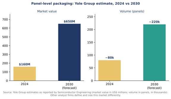
Yole Group estimates the panel-level packaging market at about $160 million in 2024, rising to roughly $650 million by 2030, which is a fourfold increase. Volume grows more slowly than value: Yole puts 2024 output at about 80,000 panels, equal to roughly 330,000 300 mm wafers, and expects nearly 220,000 panels in 2030. Those figures come from a market overview published by Semiconductor Engineering, and other research firms publish different totals because they draw the boundaries of the market differently. A separate Mordor Intelligence report puts the market at $0.44 billion in 2026 and $1.37 billion by 2031, which shows how much scope and definitions change the totals, so no single estimate should be read as a precise measure. Readers who want the technology background can start with an explainer on how the panel format differs from wafer-level processing.
Why are manufacturers moving from wafers to panels?
Manufacturers are moving to panels mainly for cost and usable area. A large square or rectangular panel lets more packages be processed in one run than a round 300 mm wafer, and Yole reports cost savings of up to 20% to 30% over fan-out wafer-level packaging in applications that need high throughput. The advantage is strongest for large dies. Yole’s analysis finds that fan-out panel-level packaging can offer cost benefits over wafer-level fan-out, especially in large-die manufacturing, although adoption depends on process maturity, yield and reliability. An overview of panel-level solutions for advanced packages describes the same logic from the organic-substrate side of the industry.
Where is panel-level packaging being adopted first?
Adoption is happening in tiers, starting with cost-driven, high-volume packages and reaching toward large, high-end ones. A Yole Group presentation at IMAPS in 2025 describes low-end and mid-end panel-level packaging as high-volume applications driven by cost reduction, and high-end ultra-high-density fan-out as a low-volume route for large packages in markets such as generative AI and high-performance computing. Yole’s description of its 2026 panel-level packaging report adds that the format is emerging as a cost-efficient alternative to wafer-level packaging for wafer-level chip-scale packages, fan-out and organic 2.5D interposers, and as a pathway to replace traditional packages such as leadframe-based QFN. That range explains why one market estimate has to cover very different products. The 2022 presentation also said adoption in ultra-high-density fan-out would be driven mainly by the large-package trend and cost benefit, and would depend on technology maturity, yield and reliability.
Which panel sizes does the industry use?
There is no single panel size. Panels in use range from 310 by 310 mm to 700 by 700 mm, and the choice depends on the application and on where the manufacturer comes from. Substrate makers tend to favor 515 by 510 mm, while a smaller 415 by 510 mm format is used in medical and industrial displays. Newer entrants from the display and printed circuit board worlds help explain the variety. Reporting on SEMI’s 3D20 standards describes them as a framework for panel characteristics that lets equipment makers design compatible tools, but adoption is still at an early stage, and dimensions today run from about 650 by 650 mm down to 400 by 500 mm. A second Semiconductor Engineering report on fan-out panel-level packaging covers the standardization question in more detail.
Which materials and players are involved?
Panel-level packaging uses organic epoxy-glass laminate and glass panels as alternatives to a silicon base, and the players come from several industries. Panels are also used to manufacture substrates for advanced packaging, and the new entrants from the display and printed circuit board worlds bring existing know-how with large formats. Yole’s 2022 trend presentation noted that glass panel lines built for the LCD industry have reached very large sizes, and that older-generation lines could be large enough to address packaging. That overlap with other panel-based industries is a large part of why equipment and standards are still settling.
What are the main hurdles for panel-level packaging?
The main hurdles are the lack of a standard panel size, the complexity of the process and the need for inspection that keeps pace with finer features. Larger packages, multiple chiplets in one package, lower interconnect pitches, smaller redistribution layer line and space, and higher layer counts all raise the difficulty for panel manufacturers. Fan-out panel-level packaging typically uses a chip-last process, which creates the need to confirm that each panel is known-good before costly dies are committed. Equipment makers face their own challenge when panel dimensions vary, because tools built for one format may not fit another.
Where does the panel format fit as AI and chiplets reshape packages?
Panel-level packaging is moving from small, low-cost chips toward AI and high-performance computing as package sizes reach 80 by 80 mm and beyond. A Yole analysis of inspection and metrology reports that panel form factors from 310 by 310 mm to 600 by 600 mm are being developed for such packages, and that TSMC has said panels will complement its CoWoS approach rather than replace it for some very large packages. The Yole report on inspection and metrology for fan-out panel packaging gives the detail behind those points.
The panel idea also reaches mainstream package types. PCB Technologies performs panel-level IC assembly, in which multiple ICs are assembled at the same time on a larger substrate rather than individually, and it has developed a panel-to-panel sealing process for packages such as QFN. Panels are therefore not limited to high-end AI hardware.
What should readers watch over the next few years?
Four indicators will show whether panel-level packaging keeps pace with its forecasts:
- Standardization: whether SEMI’s panel standards move from early adoption to common practice.
- Yield and inspection: whether known-good panel inspection keeps up with finer redistribution layers.
- Large-package adoption: how panels are used for AI and high-performance computing packages alongside existing approaches.
- Equipment convergence: whether tool makers settle on fewer panel formats.
- Forecast revisions: whether analyst estimates converge as definitions of the market become more consistent.
Frequently Asked Questions
What is panel-level packaging?
Panel-level packaging is a semiconductor packaging approach that processes many packages at once on a large rectangular or square panel instead of a round wafer.
How big is the panel-level packaging market?
Yole Group estimates the market at about $160 million in 2024 and roughly $650 million by 2030, though other analyst firms publish different figures.
Is panel-level packaging cheaper than wafer-level packaging?
It can be, since Yole reports savings of up to 20% to 30% over fan-out wafer-level packaging for high-throughput applications, but results depend on yield, package size and process maturity.
Will panels replace wafers in advanced packaging?
Not entirely, because TSMC has said panel formats will complement its CoWoS approach rather than replace it for some very large packages.
