
What actually makes a PCB “high density interconnect”?
High density interconnect PCBs are defined by their ability to pack substantially more functionality into a smaller footprint than a conventional board design allows. PCB Technologies’ HDI design guide outlines the specific manufacturing processes involved: laser drilling, using CO2 and UV lasers for precise via formation; sequential lamination, involving multiple lamination cycles to build high-layer-count boards; copper deposition, ensuring strong and reliable electrical connections; and high-resolution imaging, used for fine-line and microvia patterning. Together, these processes let designers achieve the trace density and via miniaturization that conventional PCB fabrication simply can’t support.
Why has HDI construction become essential across so many industries?
The demand for HDI construction traces back to a simple, persistent trend: electronic devices keep shrinking while their functionality keeps expanding, and HDI is one of the primary PCB-level responses to that pressure. In telecommunications equipment specifically, miniaturization and density matter directly: multi-layer PCBs, HDI technology, and the use of blind, buried, or micro vias allow more components and complex circuitry to be packed into a smaller, more compact space, which is essential for both ever-slimmer consumer devices and increasingly complex communication network equipment operating at higher frequencies.
What is a QFN package, and how does its design actually work?
QFN, or Quad Flat No-lead, is a specific IC packaging solution characterized by a leadless design, encapsulating a semiconductor die fully within a plastic package rather than exposing external leads. iNPACK’s overview of QFN IC packages describes the I/O design directly: like other QFN packages, organic QFNs use a pad-based I/O design where the semiconductor die attaches to a center pad structure, with signal I/Os arranged in a grid pattern around the package’s periphery. That leadless, pad-based construction gives QFN packages good mechanical protection for the die inside while keeping the overall package footprint compact.
How do QFN packages actually get manufactured?
QFN manufacturing increasingly relies on panel-level assembly rather than processing devices individually. iNPACK’s explanation of Panel-Level Assembly (PLA) describes this directly: PLA involves fabricating and assembling multiple ICs simultaneously on a larger substrate known as a panel, rather than individually on smaller wafers, an approach that supports optimal design and manufacturability. A panel-to-panel sealing method, based on prepregs and B-stage epoxy, can also achieve near-hermetic sealing packaging qualities, providing a level of moisture protection and environmental isolation that approaches, without fully attaining, complete hermeticity.
What options exist within the QFN packaging category itself?
| QFN option | What distinguishes it |
|---|---|
| Ceramic QFN | Higher thermal performance and reliability, typically at a higher manufacturing cost. |
| Organic QFN | Plastic-encapsulated laminate panel construction, offering flexibility in dielectric and CTE material options. |
| Lead frame QFN | A more traditional construction approach with its own tradeoffs in cost and manufacturability. |
| Multilayer QFN | Additional design flexibility, including embedded coins and hybrid construction substrates for improved performance. |
The choice between ceramic, organic, or lead frame QFN packages requires a careful, balanced approach, weighing thermal performance, cost, manufacturability, and reliability against the specific requirements of a given project. There’s no universally correct option; each package type carries distinct advantages that should be evaluated during the design phase against the application’s actual operating conditions.
How large is demand for HDI construction becoming?
The scale of investment in HDI-specific manufacturing capability continues to grow steadily. IMARC Group’s HDI PCB market analysis values the global market at $8.7 billion in 2023, projected to reach $13.4 billion by 2032, a compound annual growth rate of 4.8%. The report attributes this growth to rising demand for compact, high-performance electronics, with features like reduced size, enhanced electrical performance, and multi-layered structures making HDI PCBs increasingly essential for smartphones, automotive systems, and medical devices alike.
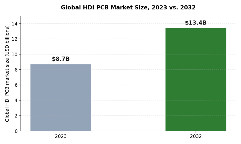
Global HDI PCB market size, 2023 versus 2032, according to IMARC Group.
Where do HDI PCBs and QFN packages actually intersect in a real design?
- Space-constrained defense and drone electronics: HDI substrates paired with QFN-packaged components maximize functionality per unit area.
- Automotive control modules: HDI’s fine traces and QFN’s compact footprint both support the size and weight targets automotive electronics demand.
- Telecom and network infrastructure: high-frequency signal integrity benefits from both HDI routing precision and QFN’s low-inductance leadless connections.
- Medical devices: miniaturization pressure in implantable and wearable devices favors combining both technologies wherever reliability standards allow.
What testing considerations actually matter once HDI PCBs and QFN packages are combined?
Combining fine-pitch HDI routing with leadless QFN packages raises the bar for inspection and testing compared to either technology used alone. Automated Optical Inspection (AOI) becomes essential for verifying circuit accuracy and detecting defects across the dense trace patterns HDI construction produces, since manual inspection simply cannot reliably catch defects at that scale. QFN packages add their own testing challenge: because the package is leadless, visually confirming solder joint quality underneath the package is far harder than with a traditional leaded component, which is why X-ray inspection and electrical testing become more important verification steps rather than optional extras. Building these testing steps into the process from the start, rather than treating them as an afterthought, is what actually keeps defect rates low as designs push both technologies toward their practical limits.
How do HDI layer counts actually map to design complexity?
Not every HDI design needs the same level of construction complexity, and matching layer count to actual design requirements avoids paying for capability a project doesn’t need. Simpler HDI designs, often described in shorthand as 1+N+1 construction, add a single sequential lamination pass on each side of a conventional core, a modest step up from standard multilayer construction. More demanding designs move to 2+N+2 or 3+N+3 construction, each additional number representing another round of laser drilling and lamination, adding cost and manufacturing time but enabling correspondingly higher trace density and connection counts. Selecting the right construction level starts with the actual routing challenge a design presents, not with defaulting to the most advanced option available, since over-specifying HDI complexity adds expense without a corresponding functional benefit.
What packaging trends are shaping how QFN is used going forward?
QFN packaging continues to evolve alongside the broader push toward smaller, more densely populated boards. Multilayer QFN designs, incorporating embedded coins and hybrid construction substrates, are increasingly used where a standard single-layer QFN can’t deliver the thermal or electrical performance a demanding application requires. At the same time, panel-level assembly techniques continue to mature, extending the cost and footprint advantages already associated with QFN packaging to increasingly complex package configurations. As HDI PCBs themselves continue trending toward higher layer counts and finer geometries, QFN packaging technology is evolving in step, since a board capable of extreme trace density gains little if the components mounted on it can’t match that same level of miniaturization.
Frequently Asked Questions
Is an HDI PCB always more expensive than a conventional PCB?
Generally yes, due to the additional laser drilling, sequential lamination, and high-resolution imaging steps involved, but that added cost is typically justified when a design’s size, weight, or performance requirements genuinely demand HDI-level trace density.
What’s the main advantage of a QFN package over a leaded package?
A QFN’s leadless, pad-based design offers a smaller footprint and can support better electrical performance at high frequencies compared to a traditional leaded package, though it also requires more precise assembly processes.
Can a QFN package be mounted on an HDI PCB?
Yes, QFN packages are commonly used on HDI PCBs specifically because both technologies serve the same underlying goal of maximizing functional density in a constrained space.
Why do some QFN designs use ceramic instead of organic materials?
Ceramic QFN packages typically offer better thermal performance and reliability, making them preferable for applications with demanding thermal or environmental requirements, though usually at a higher manufacturing cost than organic alternatives.
