
| Key Takeaways • QFN packages are leadless and bottom-terminated, while QFP and LQFP use gull-wing leads extending from all four sides, which drives most of the practical differences between them. • Typical lead pitch runs about 0.4 to 1.0 mm for QFP, fixed 0.4/0.5/0.65/0.8 mm intervals for LQFP, and commonly 0.5 or 0.65 mm for QFN. • QFN’s exposed bottom pad generally gives it a shorter thermal path to the board than leaded QFP or LQFP alternatives. • JEDEC maintains separate registered package outlines for these families, giving designers a standardized reference for body size, pitch, and lead count. |
What is the real difference between QFN, QFP, and LQFP packages?
QFN packages have no protruding leads and instead use pads along the underside of the package plus an exposed thermal die pad, while QFP and LQFP packages use “gull wing” leads that extend outward from all four sides. That structural difference drives almost everything else: QFN’s leadless, bottom-terminated design gives it a smaller footprint and a lower profile, while QFP and LQFP’s exposed leads are easier to inspect visually and easier to hand-solder or rework. the QFN package specifications available here lays out the body sizes, lead counts, and material options that typically come with a leadless design.
How does lead pitch differ across quad package families?
Lead pitch (the spacing between adjacent leads or pads) commonly runs 0.4 to 1.0 mm for QFP packages, while LQFP variants are typically offered at fixed 0.4, 0.5, 0.65, or 0.8 mm intervals, and QFN packages are frequently available at 0.5 and 0.65 mm. A tighter pitch packs more I/O into a smaller footprint but raises the bar on placement accuracy and solder-paste tolerance during assembly, which is one reason design teams weigh pitch alongside lead count rather than choosing on footprint alone.
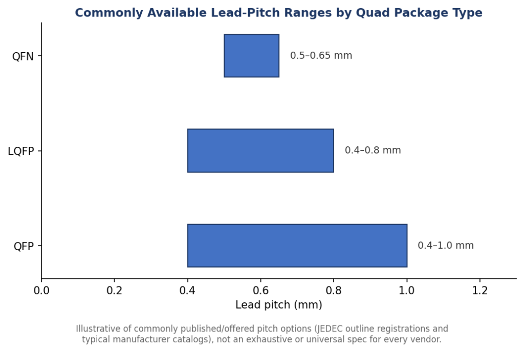
Typical lead-pitch ranges by quad package type, based on published JEDEC outline registrations and common manufacturer catalogs.
Why do QFN packages have better thermal performance than leaded alternatives?
QFN packages generally dissipate heat more effectively because the exposed die pad on the underside sits in direct contact with the PCB, giving heat a short, low-resistance path straight into the board’s copper and any thermal vias beneath it. QFP and LQFP packages rely on the leads themselves and, in some higher-power variants, an added exposed pad to move heat away from the die, which is typically a longer and less direct thermal path than a QFN’s bottom pad. a closer comparison of QFN and LGA package options walks through how material choice (ceramic, organic, or lead frame) further changes that thermal picture.
When does an LQFP make more sense than a QFN for a new design?
An LQFP is usually the better fit when a board needs visual or automated optical inspection of every solder joint, easy hand rework in low-volume or prototype builds, or a lead count and body size that a leadless footprint doesn’t comfortably support. A QFN tends to win instead when board space is tight, thermal dissipation through the board matters more than lead visibility, and the assembly line already has the reflow and inspection process (such as X-ray) needed to qualify hidden solder joints under a leadless package.
What should a design team check before committing to LQFP vs. TQFP vs. QFN?
Before locking in a package choice, a design team should confirm the target pitch and body size are actually stocked by their preferred assembly house, verify the package’s thermal resistance figures against the application’s expected power dissipation, and check whether the pin count and pitch combination is even available in the leadless format being considered. the broader IC packaging capabilities overview is a useful reference point for seeing how these package families sit alongside other packaging options such as chip-on-chip and multi-chip modules.
How do assembly and inspection costs compare between QFN and leaded packages?
QFN assembly typically costs more to verify than QFP or LQFP because a hidden, bottom-terminated solder joint can’t be checked with a simple visual or automated optical inspection (AOI) pass the way a gull-wing lead can. Most lines that run QFN in volume add X-ray inspection specifically to check for voiding under the exposed pad and to confirm the corner and side pads have wetted properly, which is an extra process step that QFP and LQFP lines can often skip or use more sparingly. That inspection overhead is one of the main reasons QFN isn’t automatically the default choice even when board space is tight — the space savings have to be weighed against the added process control needed to trust every joint on the board.
Does pin count availability differ meaningfully between these package families?
Pin count availability does differ in practice: QFP and LQFP families are generally offered across a wide span of lead counts because their leads extend outward and can be spaced more forgivingly, while QFN pin counts are more tightly linked to body size since every additional pad has to fit along the same compact perimeter. A designer choosing between a 64-pin QFN and a 64-pin LQFP for the same function will often find the QFN sits in a noticeably smaller body, but at a correspondingly tighter pitch or pad size — which loops back to the assembly-tolerance trade-off covered above rather than being a free upgrade in every case.
What do independent package-outline standards say about these formats?
JEDEC, the standards body responsible for registering microelectronic package outlines, maintains separate published outlines for QFN and QFP families, each specifying body size, pitch, and lead-count combinations that manufacturers can build against. JEDEC’s registered outline for the QFN package family and a general technical overview of quad flat package variants both confirm that QFP pitch commonly spans roughly 0.4 to 1.0 mm while LQFP is typically standardized at fixed 0.4/0.5/0.65/0.8 mm intervals — the same figures reflected in the chart above. A separate explainer on WLP, SiP, and QFN terminology, published independently here, covers how these package families relate to system-in-package and wafer-level formats.
How does package choice interact with panel-level assembly for multi-IC boards?
On boards carrying several ICs at once, package choice also affects how efficiently a panel can be populated during assembly, since a mix of leaded and leadless footprints on the same panel can force a line to run separate inspection passes rather than a single unified check. Standardizing on one package family across a board, where the design allows it, tends to simplify panel-level assembly and reduce the number of distinct process steps a line has to qualify — one reason design teams sometimes trade a marginally larger footprint for fewer package types rather than optimizing each IC’s package in isolation.
Frequently Asked Questions
Is a QFN package always smaller than a QFP with the same pin count?
Usually yes, because QFN eliminates the outward-extending leads that add to a QFP’s overall footprint, though the exact size difference depends on the specific pitch and lead count chosen.
Can QFN packages be hand-soldered for prototyping?
It’s difficult, since the leads sit underneath the package rather than along the visible edges; most prototype shops use hot-air reflow or a reflow oven with post-solder X-ray inspection instead of a hand iron.
Does a tighter lead pitch always mean a harder assembly process?
Generally yes, since tighter pitch reduces the margin for solder-paste placement and reflow alignment, which is why 0.4 mm pitch parts typically require tighter process control than 0.65 mm or 0.8 mm parts.
Are LQFP and TQFP the same package?
No — both are low-profile quad flat packages, but TQFP (thin QFP) and LQFP differ in standardized body thickness, and the two terms aren’t interchangeable even though they’re visually similar.
