In our increasingly interconnected and technology-driven lives, there’s one unsung hero that silently powers nearly every electronic device we encounter: the Printed Circuit Board. From the smartphone in your pocket and the computer on your desk to advanced medical equipment and sophisticated aerospace systems, PCBs are the foundational elements that enable electronic components to communicate and function harmoniously. They are, quite literally, the “nervous system” of modern electronics. Learn more about PCB Manufacturing processes.
What is a Printed Circuit Board?
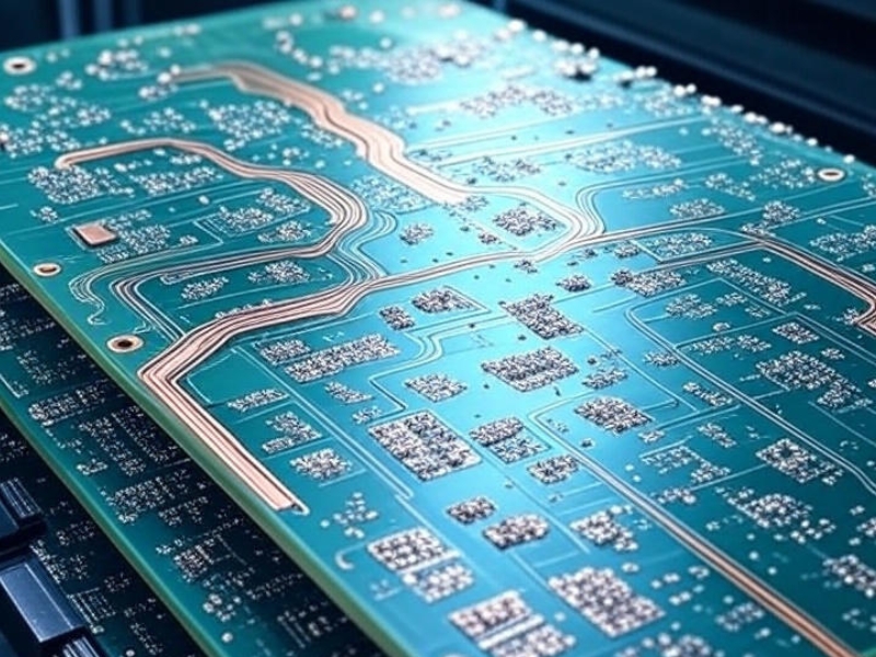
At its core, a PCB is a board that mechanically supports and electrically connects electronic components using conductive pathways, tracks, or signal traces etched from copper sheets laminated onto a non-conductive substrate. Before PCBs, electronic circuits were built using point-to-point wiring, a labor-intensive, error-prone, and space-inefficient method. The invention of the PCB revolutionized electronics manufacturing, ushering in the era of mass production and miniaturization.
Anatomy of a PCB: Layers and Materials
While PCBs come in countless variations, most share fundamental structural elements:
- Substrate (Dielectric Layer): This is the non-conductive base material that provides mechanical rigidity and electrical insulation. The most common material is FR-4 (Flame Retardant 4), a glass-reinforced epoxy laminate, known for its good balance of mechanical strength, electrical properties, and cost-effectiveness. Other materials include polyimide (for flexible PCBs), PTFE (for high-frequency applications), and ceramic.
- Copper Layers: These are the conductive pathways. Thin layers of copper foil are laminated onto the substrate. The thickness of the copper determines its current-carrying capacity. These layers are selectively etched to form the circuit traces, pads (areas for component attachment), and planes (larger areas for power or ground).
- Solder Mask: A thin, polymer layer applied over the copper traces to protect them from oxidation, corrosion, and accidental short circuits during soldering. It’s typically green but can also be red, blue, black, or other colors. It defines the areas where solder can be applied (the pads).
- Silkscreen Layer (Legend): This is a non-conductive ink layer printed on top of the solder mask. It provides labels, component designators (e.g., R1, C1), polarity indicators, and other useful information for assembly and troubleshooting. It’s usually white but can be other colors.
Types of PCBs: Adapting to Every Need
PCBs are incredibly versatile and come in several primary types, each suited for different applications:
- Single-Sided PCBs: The simplest type, with components on one side and conductive traces on the other. Used in low-cost, low-density applications (e.g., remote controls, simple calculators).
- Double-Sided PCBs: Features conductive copper layers on both sides of the substrate. Components can be placed on both sides, and holes (vias) connect traces between the layers. Common in many consumer electronics.
- Multi-Layer PCBs: Consist of more than two layers (e.g., 4, 6, 8, or even 60+ layers) of copper and substrate laminated together. Inner layers are used for signal routing, power planes, and ground planes, allowing for much higher component density and more complex circuitry (e.g., smartphones, computers, servers).
- Flexible PCBs (Flex PCBs): Built on flexible plastic substrates (like polyimide), allowing the board to bend, twist, and conform to irregular shapes. Ideal for compact, lightweight, and dynamic applications (e.g., wearables, cameras, medical implants).
- Rigid-Flex PCBs: A hybrid that combines rigid and flexible board technologies. Rigid sections support components, while flexible sections provide interconnectivity in 3D designs, eliminating the need for connectors and wires, enhancing reliability, and saving space (e.g., aerospace, advanced medical devices).
- High-Frequency PCBs: Designed with specialized low-loss dielectric materials (e.g., PTFE, ceramic-filled laminates) to handle very high-frequency signals with minimal attenuation, crucial for RF, microwave, and 5G applications.
- Metal Core PCBs (MCPCBs): Feature a metal base (often aluminum) for efficient heat dissipation, essential for high-power applications like LED lighting and power electronics.
The PCB Manufacturing Process: A Precision Craft
Manufacturing a PCB is a multi-step, highly precise process involving photolithography, chemical etching, drilling, plating, and lamination:
- Design: Engineers create the PCB layout using Electronic Design Automation (EDA) software, defining traces, pads, components, and layers.
- Film Generation: The design is transferred to photographic films, one for each layer.
- Material Preparation: Copper-clad laminates are cut to size.
- Inner Layer Processing (for multi-layer): Copper on inner layers is cleaned, laminated with a photoresist, exposed to UV light through the film (to transfer the circuit pattern), developed (removing unexposed resist), and then etched (removing unwanted copper). The remaining resist protects the desired traces.
- Lamination: For multi-layer boards, the etched inner layers, prepreg (adhesive), and outer copper foils are precisely stacked and subjected to high temperature and pressure to bond them into a solid board.
- Drilling: Holes for vias (inter-layer connections) and component leads are drilled with extreme precision, often using CNC machines or lasers.
- Plating: The drilled holes and copper surfaces are chemically plated with a thin layer of copper to create conductive paths through the holes (PTH – Plated Through-Holes).
- Outer Layer Processing: Similar to inner layers, photoresist is applied, exposed, developed, and etched to form the external traces and pads.
- Solder Mask Application: A liquid photoimageable solder mask is applied, exposed through a film to open up pad areas, and then cured.
- Silkscreen Printing: Component designators and markings are printed onto the board.
- Surface Finish: A surface finish (e.g., HASL, ENIG, OSP) is applied to the exposed copper pads to protect them from oxidation and ensure good solderability.
- Profiling/Routing: The individual PCBs are cut from the larger manufacturing panel using a router or laser.
- Electrical Test: Each PCB is electrically tested to ensure all connections are correct and there are no shorts or open circuits.
- Final Inspection: Visual inspection and packaging.
The Importance of PCBs in Modern Technology
PCBs are more than just a means to connect components; they are crucial for:
- Miniaturization: Enabling smaller, more compact electronic devices.
- Reliability: Providing stable and durable interconnections that withstand vibration and environmental stresses.
- Performance: Optimizing signal integrity for high-speed data transmission and complex circuit functionality.
- Mass Production: Facilitating automated assembly and consistent quality for high-volume manufacturing.
- Cost-Effectiveness: Reducing labor costs and improving efficiency compared to manual wiring.
From cutting-edge AI servers and autonomous vehicles to life-saving medical devices and the foundational infrastructure of the internet, Printed Circuit Boards are the invisible backbone. As technology continues to advance, demanding ever more power, speed, and miniaturization, the innovation in PCB design and manufacturing will remain at the forefront, continuing to enable the electronic wonders of our world.