Summary: As electronic devices pack more processing power into smaller spaces, thermal management has become one of the most critical – and complex – challenges in PCB design and manufacturing.
This article covers: why PCB thermal management is reaching a critical inflection point; the key market drivers intensifying the challenge; existing industry solutions; common limitations; and how advanced substrate and packaging technology provides a superior path forward for demanding applications.
For design engineers working on high-performance systems, heat is not just an inconvenience – it is a fundamental constraint that determines product reliability, longevity, and performance. Experts looking for advanced PCB heat dissipation solutions for high-performance systems will find that the field has evolved dramatically in recent years, driven by the compounding pressures of power density growth, miniaturization, and lead-free manufacturing requirements.
Why Thermal Management Has Become a Critical PCB Challenge
A decade ago, PCB thermal management was largely a second-order concern for most design teams. Standard copper pours, thermal vias, and basic heat sinking were sufficient for the majority of applications. Today, those approaches are frequently inadequate.
The combination of Moore’s Law-driven performance growth, the shift to lead-free soldering (which requires higher reflow temperatures and stresses interconnects more severely), the proliferation of multi-layer board designs, and the relentless miniaturization trend has created a fundamentally more challenging thermal environment. Power densities in advanced processors, power electronics, and RF components have increased dramatically, while the available board area for heat dissipation has shrunk.
According to the IPC – the global electronics manufacturing association – thermal failure is among the top three root causes of premature electronics failure in high-reliability applications. Managing heat is no longer an afterthought; it is a primary design discipline.
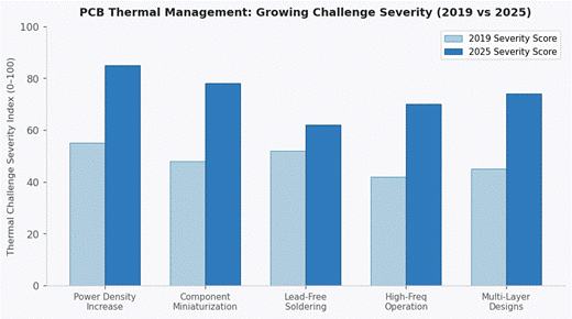
Key Market Drivers Intensifying Thermal Challenges
- Increasing Power Density: Advanced processors and FPGAs now routinely dissipate 100–300+ watts in compact packages. Multi-chip modules and 3D-stacked dies concentrate even more heat in even smaller areas, creating thermal hotspots that challenge traditional heat spreading strategies.
- High-Frequency RF and Millimeter-Wave Applications: 5G base stations, phased array radars, and automotive ADAS systems operate at frequencies where power amplifier efficiency drops and heat generation rises significantly. The RF substrate must dissipate heat efficiently without compromising dielectric properties that affect signal performance.
- Miniaturization in Medical and Wearable Devices: Implantable and wearable medical devices must manage heat within tight volume and weight constraints, while ensuring that device temperature never poses a safety risk to the patient or user. This creates a thermal design challenge with direct human health implications.
- Automotive and Industrial Temperature Extremes: Electronic control units and power modules in electric vehicles and industrial machinery must operate reliably across temperature ranges from -40°C to +150°C or beyond. Thermal cycling at these extremes stresses solder joints, substrate materials, and component attachments.
- Defense and Aerospace Reliability Requirements: Defense electronics must maintain operation under extreme environmental conditions. Thermal derating, which reserves thermal headroom to ensure reliable operation under worst-case conditions, requires that the baseline thermal performance of the PCB substrate be substantially better than the nominal operating conditions.
The PCB industry has developed a range of approaches to manage heat, each with meaningful strengths and notable limitations:
The Traditional Toolkit: What Works and Where It Falls Short
- Thermal Vias: Arrays of plated through-holes beneath hot components create conduction paths to inner ground planes and heatsinks. Effective but limited by via density, board thickness, and the thermal resistance of the via fill material.
- Metal Core PCBs (MCPCBs): An aluminum or copper core layer dramatically improves lateral heat spreading. Effective for LED lighting and power electronics, but limited in layer count, design flexibility, and compatibility with fine-pitch components.
- Thermal Interface Materials (TIMs): Thermally conductive pads and compounds reduce the contact resistance between components and heatsinks. Important but not a solution for heat generated within the substrate itself.
- Embedded Heat Spreaders: Copper or copper-molybdenum composite (CMC) coins embedded directly in the substrate provide a high-conductivity path from the die to the external heatsink. This is one of the most effective approaches for high-power applications, but requires specialized substrate manufacturing capability.
The critical limitation of most conventional approaches is that they are add-ons to standard PCB designs rather than fundamental aspects of the substrate architecture. As power densities continue to rise, these incremental solutions become insufficient, and a more holistic approach to thermal management – starting at the substrate design stage — becomes essential.
For engineers seeking a research foundation, the IPC technical resources library offers comprehensive standards and technical papers on thermal management best practices in PCB design and assembly.
Advanced Substrate Technology: The New Frontier of Thermal Management
The most effective approach to PCB thermal management today integrates thermal considerations into the substrate architecture from the earliest design stage – not as an afterthought. Advanced substrate materials and construction techniques are fundamentally changing what is possible.
PCB Technologies’ approach to thermal management, delivered through its integrated service offering and iNPACK division, addresses thermal challenges at the substrate level. Their organic substrate solutions combine advanced dielectric materials with embedded copper coin technology and controlled via fill to create thermal pathways designed specifically for high-power semiconductor packages.
Key elements of this advanced approach include:
- Embedded Coin Technology: Copper or CMC coins embedded directly beneath high-power dies provide a direct conduction path with thermal conductivity orders of magnitude higher than standard FR4 dielectric. This technique, refined through years of defense and aerospace application, is now available for a broader range of industries.
- Controlled Dielectric Selection: The choice of substrate dielectric affects not only thermal conductivity but also CTE matching, signal integrity, and mechanical stability. PCB Technologies’ materials expertise – built over more than 40 years – enables optimal dielectric selection for each specific thermal and electrical requirement.
- Via Fill and Thermal Via Arrays: Precisely engineered via fill technology, combined with optimized via array design, maximizes heat conduction from the die level through the substrate to the system heatsink.
- Thermal Simulation and DfM Integration: PCB Technologies’ Design for Manufacturing (DfM) services analyze PCB designs layer by layer, including thermal analysis, identifying thermal risk areas early in the design cycle where changes are inexpensive and effective.
The All-in-One Advantage for Thermal-Critical Applications
One of the most underappreciated factors in PCB thermal management is the gap between design intent and manufacturing reality. Thermal simulations assume ideal material properties and perfect assembly, but real-world manufacturing variations – void formation in via fills, inconsistent thermal interface material application, and substrate material lot variations – can significantly degrade thermal performance.
PCB Technologies’ integrated model, with design, fabrication, assembly, and testing under one roof, dramatically reduces this design-to-manufacturing gap. Their ISO 9001, ISO 14001, ISO 13485, and AS 9100 certifications reflect the quality management systems that ensure manufactured products meet their designed thermal specifications – not just on paper, but in production.
For applications where thermal failure is not an option – medical implants, aerospace electronics, high-power RF systems – this level of integrated quality control is not a luxury. It is a requirement.
Conclusion: Thermal Management Is a First-Principle Design Challenge
The era of treating thermal management as a late-stage PCB design task is over. Rising power densities, miniaturization pressures, and demanding application environments have elevated thermal performance to a first-principle design constraint that must be addressed at the substrate architecture level, integrated into the DfM process, and validated through rigorous test and qualification.
The most successful engineering teams in thermally demanding industries are those that engage with substrate and packaging experts early in the design process – leveraging materials knowledge, simulation expertise, and integrated manufacturing capability to build thermal performance into the foundation of their designs, rather than trying to engineer around heat after the fact.